# Raspberry Pi CM4 HAT
This page is not ready yet...
The board is designed for expand Raspberry Pi functionality:
- Connecting CAN bus
- LTE modem
- Measure internal voltages
- Able to use SWD to debug other MCUs
- Connecting over UART to PX4 over MAVLINK
CAN bus gives access to Cyphal (opens new window)/DroneCAN (opens new window) (old name UAVCAN).
# 1. General
# 1.1. Variations
There are two connection options.
| RPI CM4 | RPI4 Common |
|---|---|
 |  |
# 1.2. Main function
# 2. Hardware specification
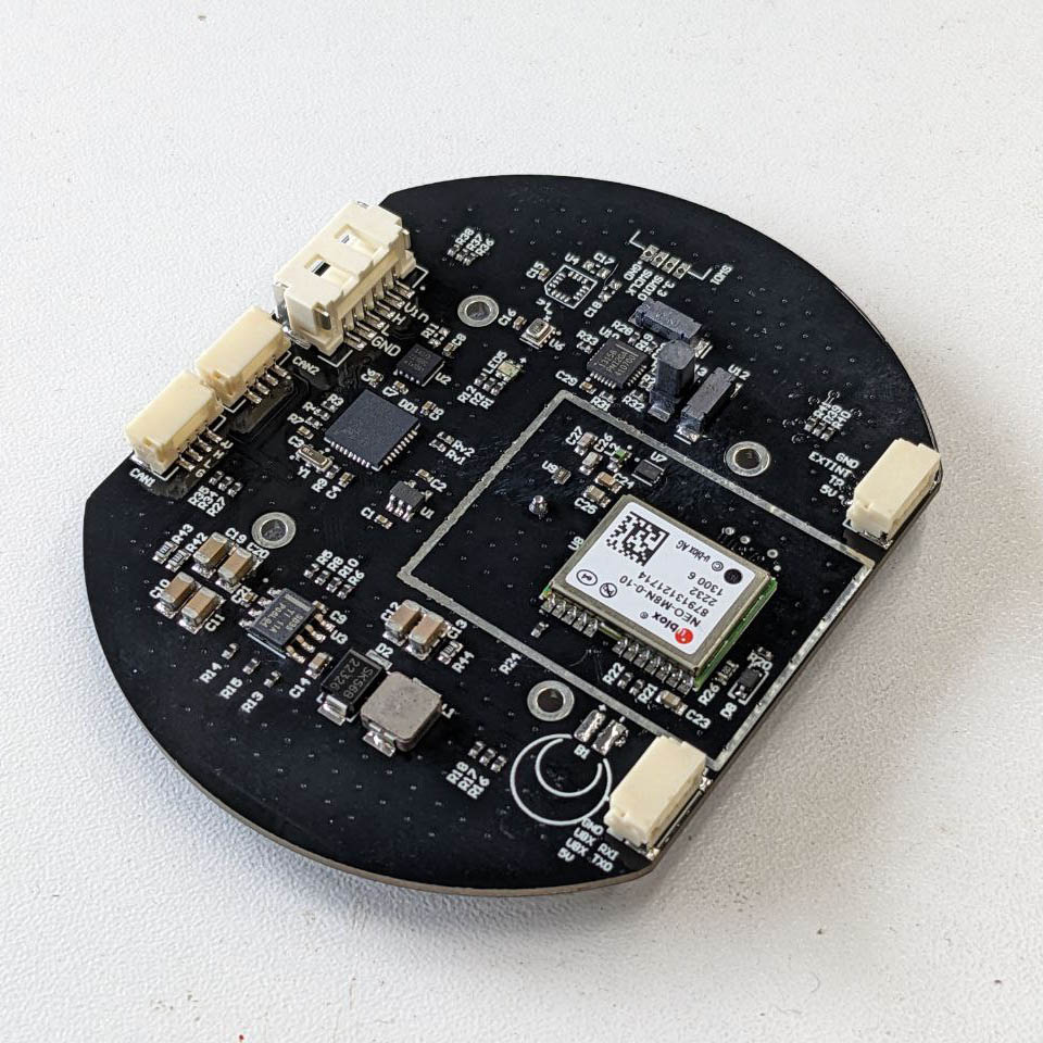
| View | Top | Bot |
|---|---|---|
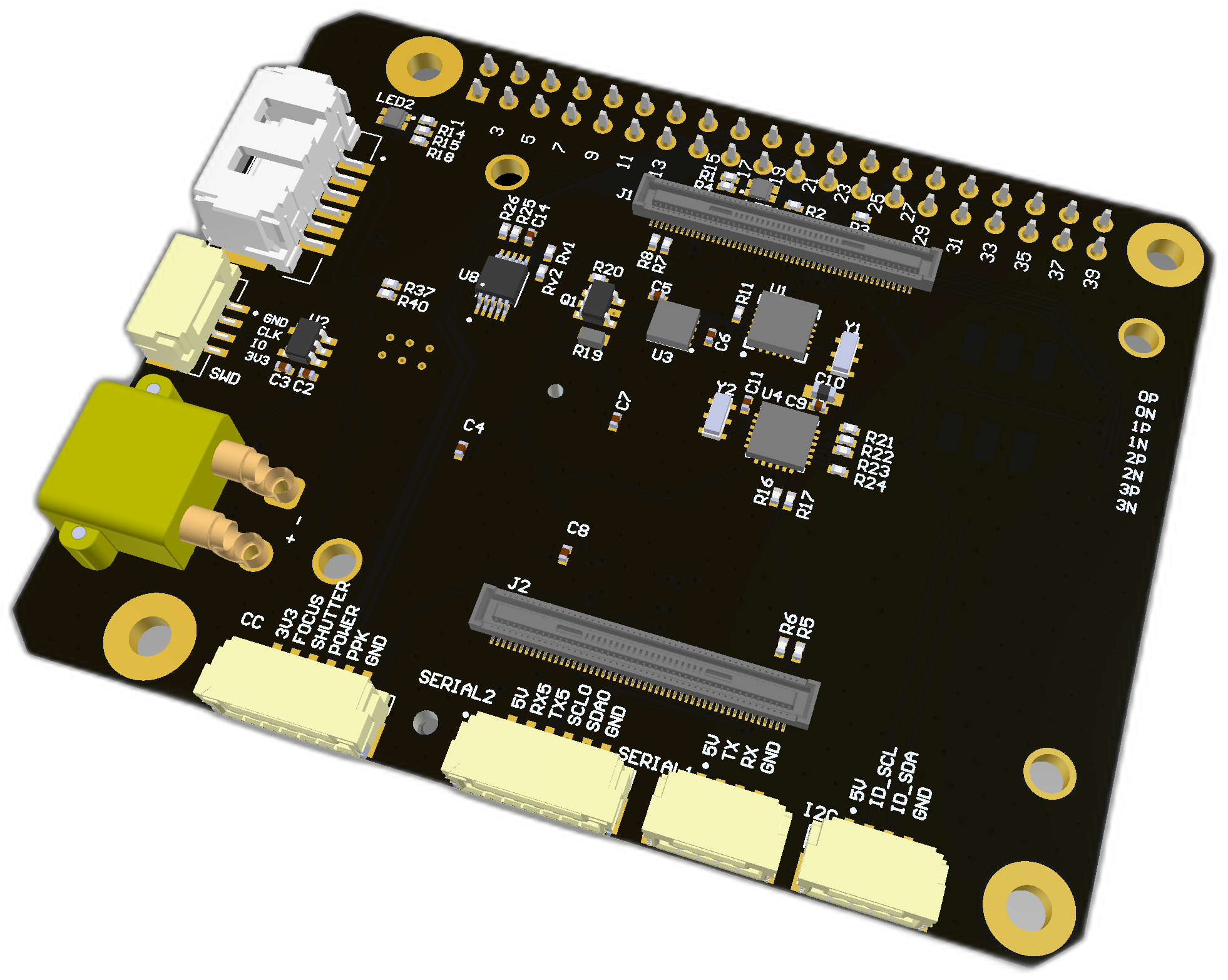 | 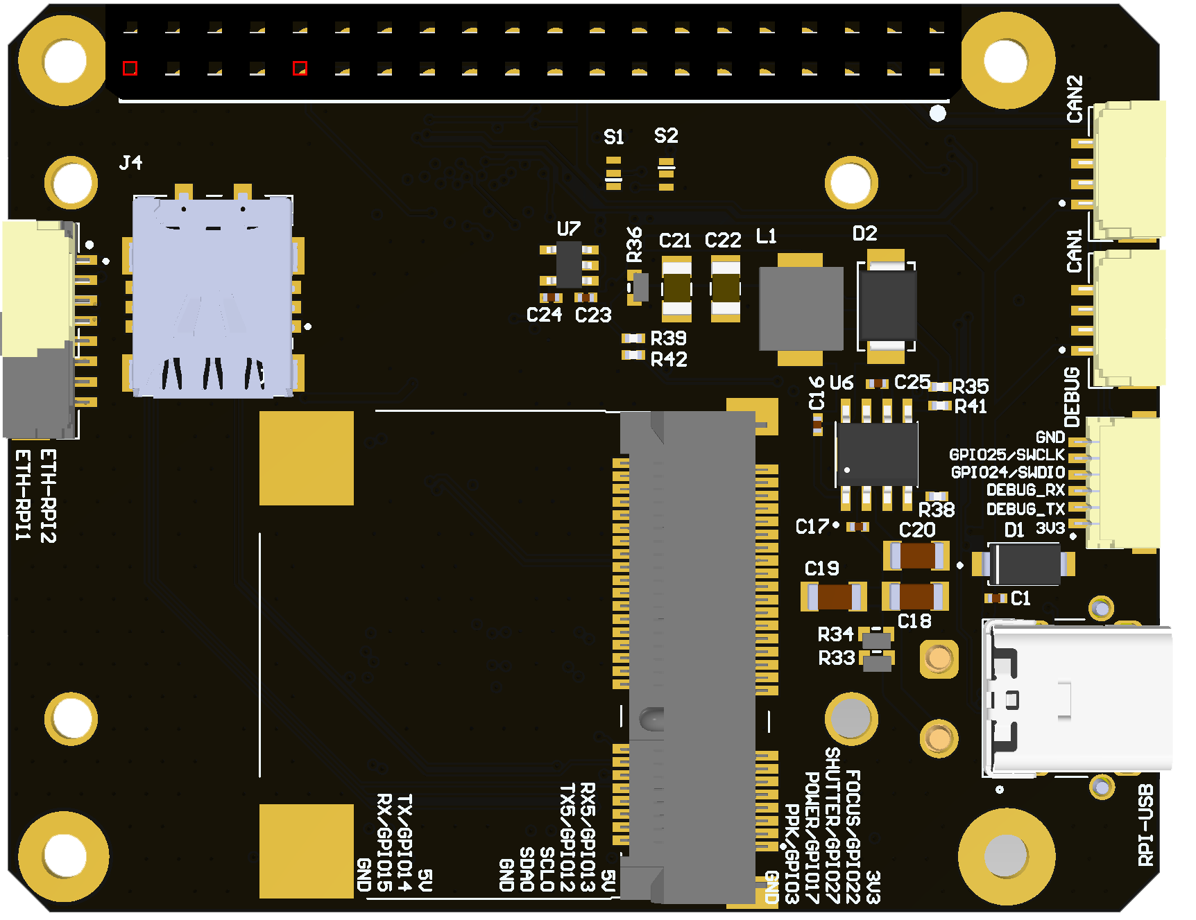 | 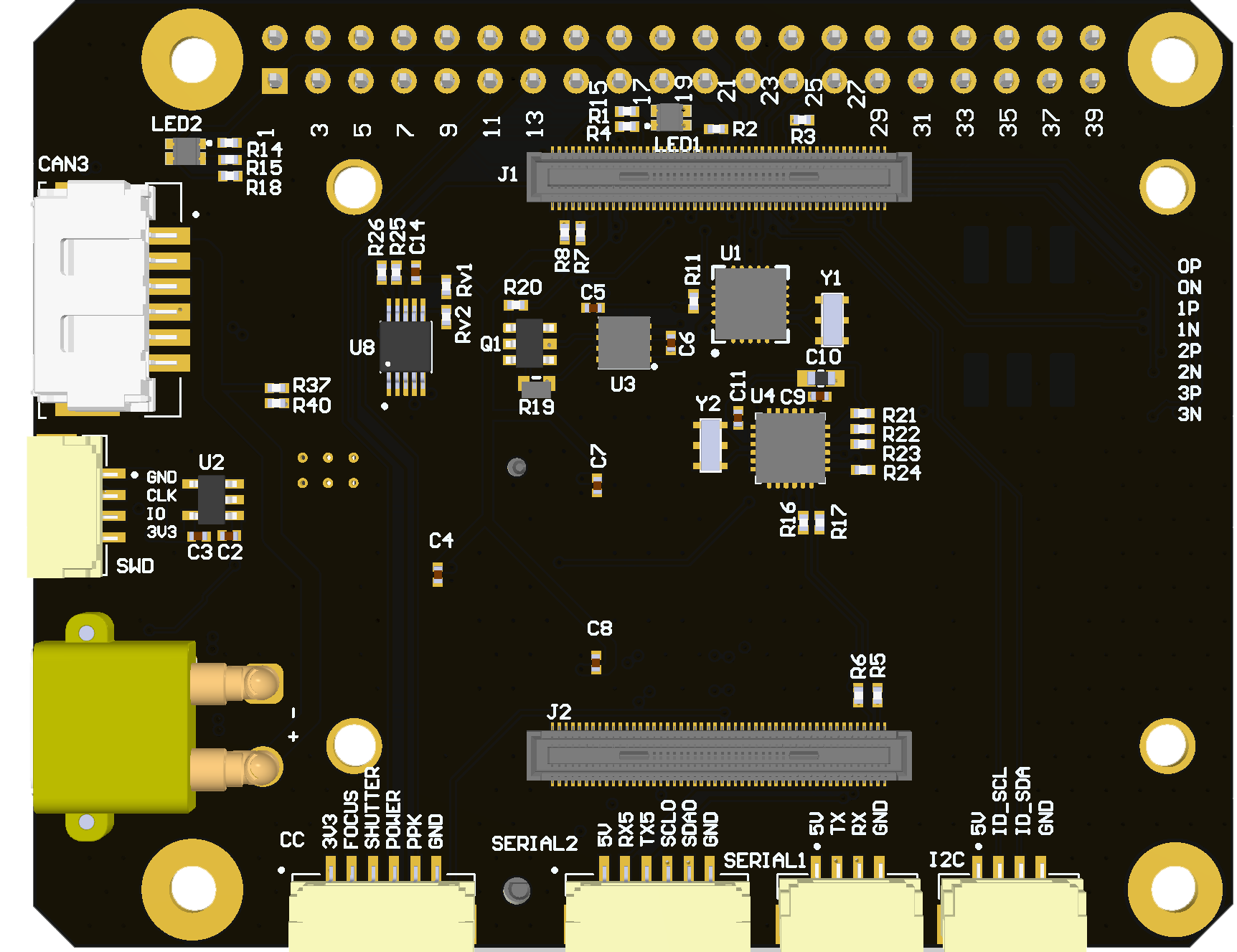 |
 |  |
# 2.1. Features
- CAN to SPI - MCP2515-I/ST
- ADC measurements ADS1115IDGSR
- LTE over USB
- SWD connector
- SERIAL conneectors
- RGB LED
# 2.2. Wire
Connectors
| № | Name | Description |
|---|---|---|
| 1 | CAN1, CAN2 | CAN port |
| 3 | SWD | Serial wire debug from RPI to STM |
| 4 | DEBUG | SWD |
| 6 | XT30PW-M | Power input |
| 8 | SERIAL1 | RPI ttyS0 |
| 12 | RPI-USB | RPI USB Type-C |
| 14 | J5 | Ethernet RJ45 connected to RPI |
Pin configuration and functions
Pin configuration for RPI
| GPIO | Defedition | Comment |
|---|---|---|
| GPIO0 | ID_SDA - SDA0,SDA6 | I2C connector |
| GPIO1 | ID_SCL - SCL0,SCL6 | I2C connector |
| GPIO2 | ||
| GPIO3 | CC_PPK | SCL1? |
| GPIO4 | PI_TX3 | DEBUG_TX |
| GPIO5 | PI_RX3 | DEBUG_RX |
| GPIO6 | ||
| GPIO7 | ||
| GPIO8 | MCP2515_nCS | |
| GPIO9 | MCP2515_MISO | |
| GPIO10 | MCP2515_MOSI | |
| GPIO11 | MCP2515_SCK | |
| GPIO12 | MCP2515_INT | TODO: Check if it can be movied out |
| GPIO12 | RPI_TX5 | SERIAL2(3) |
| GPIO13 | RPI_RX5 | SERIAL2(2) |
| GPIO14 | PI_TXO | SERIAL1 |
| GPIO15 | PI_RXI | SERIAL1 |
| GPIO16 | BLUE LED | |
| GPIO17 | CC_POWER | |
| GPIO18 | GREEN LED | LED1 |
| GPIO19 | ||
| GPIO20 | GREEN LED | |
| GPIO21 | RED LED | |
| GPIO22 | CC_FOCUS | SDA6? |
| GPIO23 | ||
| GPIO24 | SWDIO ? | SWD and DEBUG connector |
| GPIO25 | SWCLK ? | SWD and DEBUG connector |
| GPIO26 | ||
| GPIO27 | CC_SHUTTER | SCL6? |
| GPIO44 | I2C SDA0,SDA1 | ADS1115IDGSR and SERIAL2(5) |
| GPIO45 | I2C SCL0,SCL1 | ADS1115IDGSR and SERIAL2(4) |

RPI UART map (opens new window)
| TXD | RXD | CTS | RTS | Comment | |
|---|---|---|---|---|---|
| uart0 | 14 | 15 | 8 | 10 | SERIAL1 |
| uart1 | 14 | 15 | 8 | 10 | Occupied by SERIAL1 |
| uart2 | 0 | 1 | 2 | 3 | Occupied by I2C6 or I2C0 |
| uart3 | 4 | 5 | 6 | 7 | DEBUG |
| uart4 | 8 | 9 | 10 | 11 | Occupied by SPI0 |
| uart5 | 12 | 13 | 14 | 15 | SERIAL2 |
# CAN-SPI interface MCP2515 PINOUT
| RP4 HEADR | RP4 GPIO | SIGNAL | MCP2515 TJA1050 MODULE |
|---|---|---|---|
| #01 | Power | 3.3V | VCC |
| #02 | Power | 5V | Extra wire to TJA1050 VCC |
| #06 | Power | GND | GND |
| #09 | Power | GND | GND to CAN BUS (there is no GND terminal on CAN MODULE) |
| #19 | GPIO 10 | MOSI | SI |
| #21 | GPIO 9 | MISO | SO |
| #23 | GPIO 11 | SCLK | SCK/CLK |
| #24 | GPIO 8 | SPI0.CE0 | CS |
| #32 | GPIO 12 | INT | INT |
# LED
| GPIO | Defedition | Comment |
|---|---|---|
| GPIO18 | GREEN LED | LED1 |
| GPIO16 | BLUE LED | |
| GPIO20 | GREEN LED | |
| GPIO21 | RED LED |
# ADC ADS1115IDGSR
| GPIO | Defedition | Comment |
|---|---|---|
| GPIO45 | I2C SCL0,SCL1 | ADS1115IDGSR and SERIAL2(4) |
| GPIO44 | I2C SDA0,SDA1 | ADS1115IDGSR and SERIAL2(5) |
# USB HUB, LTE MODEM, Type-C port
Terminus Tech FE1.1S-BQFN24B (opens new window) connected to RPI USB port.
# 2.3. Specifications
Mechanical
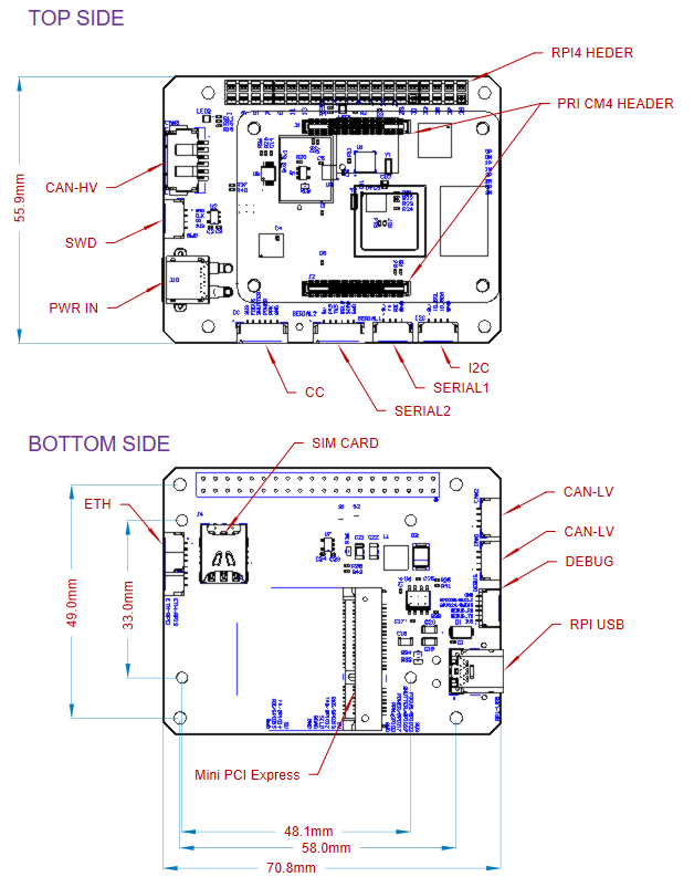
| Width, mm | Length, mm | Height, mm | |
|---|---|---|---|
| Outline | 70.8 | 55.9 | 1.6 |
| PCB | 70.8 | 55.9 | 16.7 |
Total weight of device is XXXXXX g.
You can download 3D model on GrabCAD (opens new window)
Housing
Information about case presented here.
Absolute Maximum Ratings
| Parameter | MIN | MAX | UNIT |
|---|---|---|---|
| Vin (CAN1) | 5.5 | 55* | V |
| V (CAN2, CAN3) | 4.5 | 5.5 | V |
| I max | A | ||
| Operating temperature |
*Noted Voltage should be delivered only with current limitation under 2.5 Amp.
Recommended operating conditions
| Parameter | Value | UNIT |
|---|---|---|
| Vin (CAN3) | 30 | V |
| V (CAN1, CAN2) | 5 | V |
| I max | A |
ESD ratings
| Description | Value | UNIT |
|---|---|---|
| Human-body model (HBM) | 2000 | V |
| Charged-device model (CDM) | 500 | V |
# 2.4. Description
Functional Block Diagram
Connection example diagram
# 2.5. Power Supply Recommendations
Device is designed to operate from an input voltage supply range between 4.5 V and 5.5 V over CAN2 or CAN3 connector, or 5.5 - 30 V from CAN1. This input supply must be able to withstand the maximum input current and maintain a stable voltage. The resistance of the input supply rail should be low enough that an input current transient does not cause a high enough drop that can cause a false UVLO fault triggering and system reset. The amount of bulk capacitance is not critical, but a 47-μF or 100-μF electrolytic capacitor is a typical choice.
# Applications
# 2. Led indication
- LED1
- PI_LED_nPWR - RED
- GPIO18 - GREEN
- PI_nLED_Activity - BLUE
# Useful links:
- cm4io datasheet (opens new window)
- cm4 datasheet (opens new window)
- waveshare.com/cm4-nano-a.htm (opens new window)
- raspberrypi.stackexchange.com/questions/104464/where-are-the-uarts-on-the-raspberry-pi-4 (opens new window)
# Useful links about RPI:
# Inspired by
- waveshare.com/rs485-can-hat.htm (opens new window)
- waveshare.com/wiki/RS485_CAN_HAT (opens new window)
- waveshare.com/wiki/File:RS485_CAN_HAT_Schematic.pdf (opens new window)
# 2.6. Revision history
| version | Description |
|---|---|
| v |