# 4. MAGNETOMETER RM3100
| View | Top | Bottom |
|---|---|---|
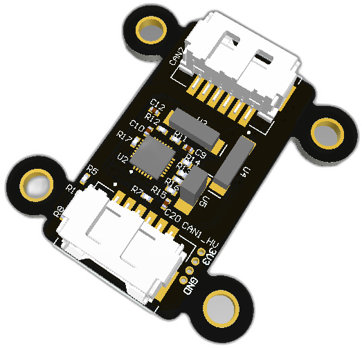 | 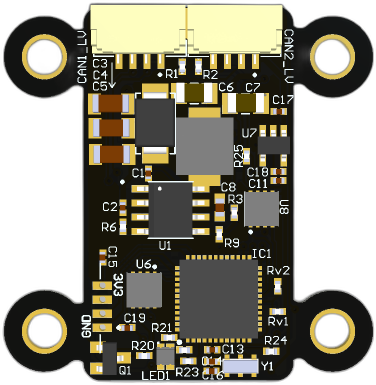 | 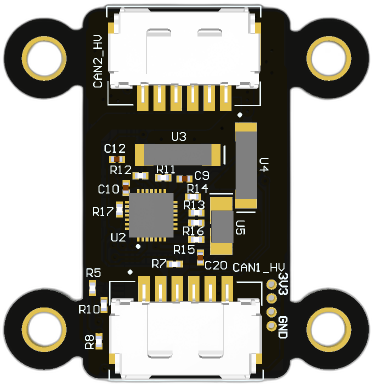 |
# 4.1. Features
# 4.2. Wiring
Schematic features. Schematic can be provided via issue.
Connectors
The node has connectors which are described in the table below.
| N | Connector | Description |
|---|---|---|
| 1 | CAN1_HV, CAN2_HV | |
| 2 | CAN1_LV | |
| 3 | CAN2_LV | |
| 4 | SWD1 |
Here (opens new window) you can find manufacturer part number of connectors it self and its mates.
Pin configuration and functions
| Pin N | CAN1_HV | Pin N | CAN2_HV | Pin N | CAN1_LV | Pin N | CAN2_LV | Pin N | SWD1 |
|---|---|---|---|---|---|---|---|---|---|
| 1 | Vin | 1 | Vin | 1 | 5V | 1 | 5V | 1 | GND |
| 2 | Vin | 2 | Vin | 2 | FDCAN1_H | 2 | FDCAN2_H | 2 | SWLK |
| 3 | FDCAN1_H | 3 | FDCAN2_H | 3 | FDCAN1_L | 3 | FDCAN2_L | 3 | SWDIO |
| 4 | FDCAN1_L | 4 | FDCAN2_L | 4 | GND | 4 | GND | 4 | 3.3 |
| 5 | GND | 5 | GND | SH1 | GND | SH1 | GND | ||
| 6 | GND | 6 | GND | SH2 | GND | SH2 | GND | ||
| P1 | GND | P1 | GND | ||||||
| P2 | GND | P2 | GND |
Here you can see all connections of MCU.
| MCU PIN | PIN Numer | NET Name | Description |
|---|---|---|---|
| PA7 | 18 | VERSION | |
| PA5 | 16 | TX_READY | |
| PD3 | 41 | TX5 | |
| PA9 | 29 | TX | |
| PC7 | 31 | TIMEPULSE | |
| PA14-BOOT0 | 36 | SWLK | |
| PA13 | 35 | SWDIO | |
| PA12_[PA10] | 34 | STM_USB_DP | |
| PA11_[PA9] | 33 | STM_USB_DM | |
| PF2-NRST | 10 | STM_NRST | |
| PB7 | 46 | SDA/PWM4B | |
| PB6 | 45 | SCL/PWM4A | |
| PB13 | 25 | SCK/ADC_VB | |
| PD2 | 40 | RX5 | |
| PA10 | 32 | RX | |
| PC6 | 30 | RTK | |
| PB8 | 47 | PWM3B | |
| PB9 | 48 | PWM3A | |
| PB5 | 44 | PWM3_2 | |
| PB4 | 43 | PWM3_1 | |
| PB15 | 27 | PB15 | |
| PB10 | 22 | PB10 | |
| PB3 | 42 | PB3 | |
| PB2 | 21 | PB2 | |
| PA15 | 37 | PA15 | |
| PF1-OSC_OUT | 9 | OSC_OUT | |
| PF0-OSC_IN | 8 | OSC_IN | |
| PB12 | 24 | NSS/ADC_VA | |
| PA2 | 13 | nRESET | |
| PB11 | 23 | MOSI/ADC_MID | |
| PB14 | 26 | MISO/ADC_VC | |
| PC13 | 1 | LED3 | |
| PC15-OSC32_OUT | 3 | LED1 | |
| PC14-OSC32_IN | 2 | LED | |
| VSS/VSSA | 7 | GND | |
| VSS | 49 | GND | |
| PA8 | 28 | GEO | |
| PB1 | 20 | FDCAN2_TX | |
| PB0 | 19 | FDCAN2_RX | |
| PD1 | 39 | FDCAN1_TX | |
| PD0 | 38 | FDCAN1_RX | |
| PA4 | 15 | EXTINT | |
| PA3 | 14 | ANT_DETECT | |
| PA0 | 11 | ADC_VIN | |
| PA6 | 17 | ADC_CUR | |
| PA1 | 12 | ADC_5V | |
| VBAT | 4 | 3.3 | |
| VREF+ | 5 | 3.3 | |
| VDD/VDDA | 6 | 3.3 |
# 4.3. Specifications
Mechanical
Scheme is shown on the picture below. CAN model can be provided via email request or issue on github or downloaded on GrabCAD (opens new window).
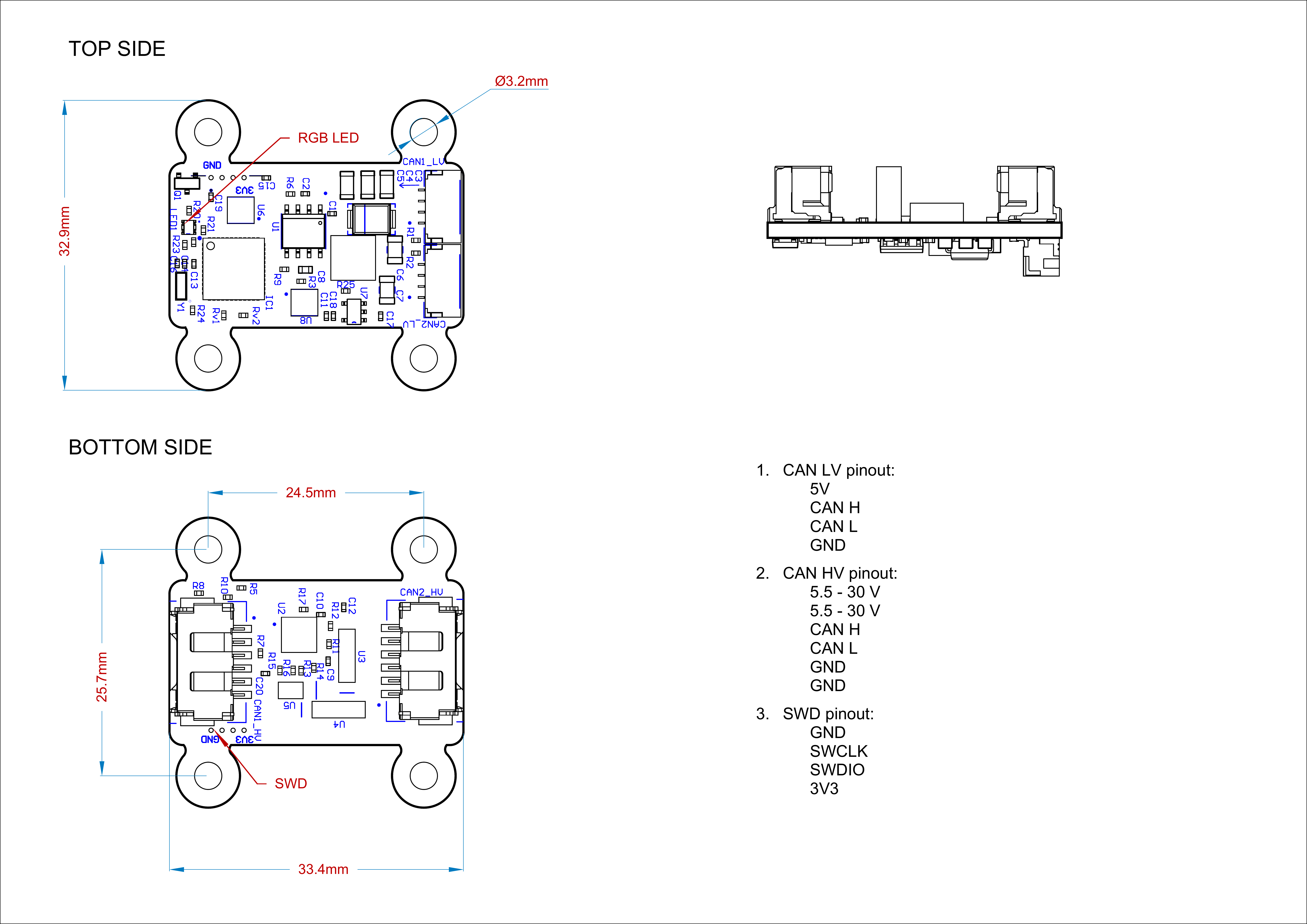
| Width, mm | Length, mm | Height, mm | |
|---|---|---|---|
| Outline | 25.7 | 33.4 | 12.5 |
| PCB | 21.29 | 33.4 | 1.6 |
Total weight of device less than 50 g.
# Housing
Information about case presented here.
# Absolute Maximum Ratings
# Recommended operating conditions
# ESD ratings
# MTFF
# 4.4. Integration
Recommended mechanical mounting
Connection example diagram
# 4.5. Power Supply Recommendations
Device is designed to operate from an input voltage supply range between 4.5 V and 5.5 V over CAN2 or CAN3 connector, or 5.5 - 30 V from CAN1. This input supply must be able to withstand the maximum input current and maintain a stable voltage. The resistance of the input supply rail should be low enough that an input current transient does not cause a high enough drop that can cause a false UVLO fault triggering and system reset. The amount of bulk capacitance is not critical, but a 47-uF or 100-uF electrolytic capacitor is a typical choice.
# 4.6. Revision history
| View | Version | Date | Description |
|---|