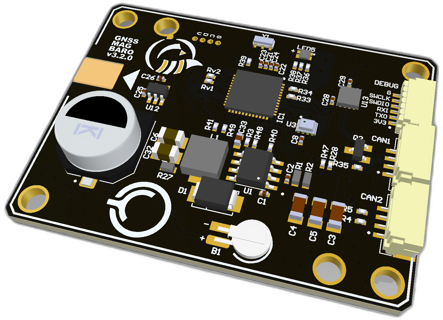
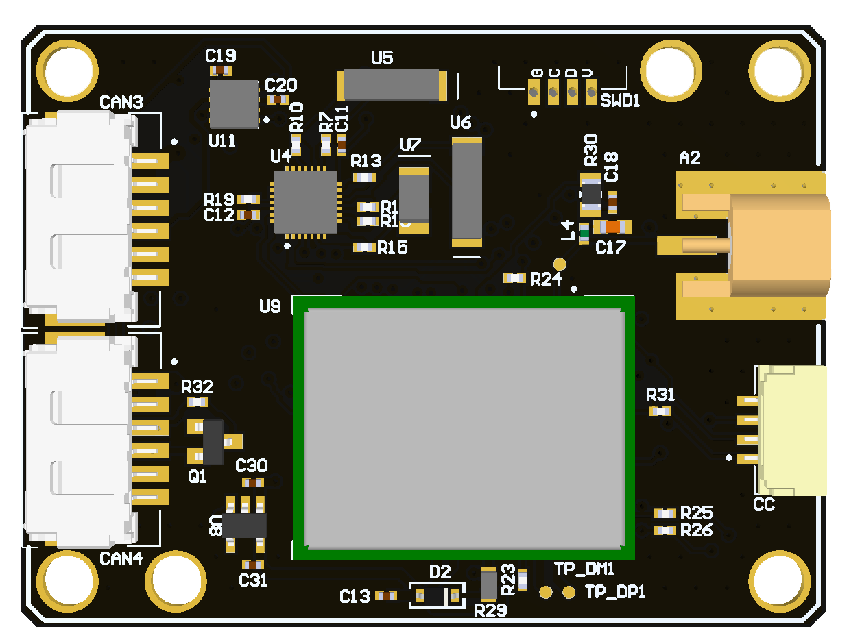
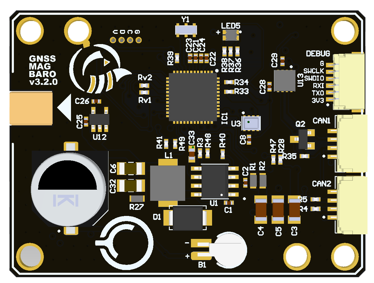
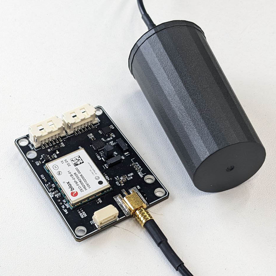
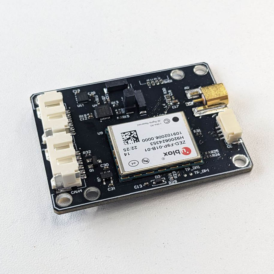
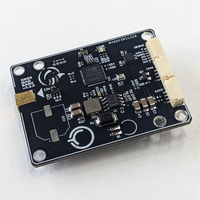
# 3. V3.2 GNSS (ZED-F9P) MAG BARO with EXTERNAL ANTENNA hardware
Multi-band GNSS receiver delivers centimeter level accuracy in seconds.
The ZED-F9P positioning multi-band GNSS and real time kinematics (RTK) technology in a compact form factor, to deliver centimeter-level accuracies in seconds for the industrial navigation and robotics markets. ZED-F9P concurrently uses GNSS signals from all four GNSS constellations (GPS, GLONASS, Galileo, and BeiDou). GNSS signals from multiple frequency bands (L1/L2) combined with RTK technology enables fast convergence times and reliable performance for scalable applications, including robotic lawnmowers, unmanned autonomous vehicles (UAV), and semi-automated or fully automated machinery.
| View | Top | Bottom |
|---|---|---|
 |  |  |
 |  |  |
# 3.1. Features
- Concurrent reception of GPS, GLONASS, Galileo and BeiDou
- Multi-band RTK with fast convergence times and reliable performance
- Centimeter-level accuracy in a small and energy-efficient module
- Easy integration of RTK for fast time-to-market
- Magnetometer RM3100 (opens new window)
- Baro BMP280
- 2 CAN
- 2 JST SM04B connectors compatible with Dronecode Autopilot Connector Standard (opens new window)
- 1 MOLEX (opens new window) non standart connector
- GNSS module ZED-F9P (opens new window) (Datasheet (opens new window) and Interface Description (opens new window))
- External antenna MCX connector
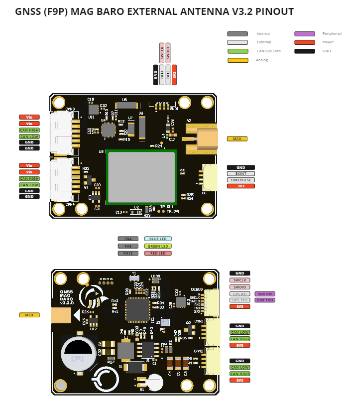
# 3.2. Wire
Schematic features. Schematic can be provided via issue.
Connectors
The node has 3 connectors which are described in the table below.
| № | Connector | Description |
|---|---|---|
| 1 | CAN1, CAN2 | Devices that deliver power to the bus are required to provide 4.5–5.5 V on the bus power line, 5.0 V nominal. Devices that are powered from the bus should expect 4.5–5.5 V on the bus power line. The current shall not exceed 1 A per connector. |
| 2 | CAN3, CNA4 | Can be powered from 5.5 to 30 volts and connected to CAN bus |
| 3 | SWD | STM32 firmware updating using programmer-sniffer. |
| 4 | DEBUG | Debug connector matches with Zubax probe (opens new window) |
| 5 | CC | Camera capture port can be used to receive external interrupt from camera trigger and send timepulse to payload such as autopilot |
| 6 | MCX | To be used with external active antenna |
Here (opens new window) you can find manufacturer part number of connectors it self and its mates.
Pin configuration and functions
| Pin | CAN3, CAN4 | DEBUG | Pin | CAN1, CAN2 | SWD | CC |
|---|---|---|---|---|---|---|
| 1 | Vin | 3.3V | 1 | 5V in | GND | 3.3V |
| 2 | Vin | GPS TXO | 2 | CAN High | SWCLK | TIMEPULSE |
| 3 | CAN High | GPS RXI | 3 | CAN Low | SWDIO | EXTINT |
| 4 | CAN Low | SWDIO | 4 | GND | 3.3V | GND |
| 5 | GND | SWCLK | ||||
| 6 | GND | GND |
Here you can see all connections of MCU.
| MCU PIN | PIN Numer | NET Name | Description |
|---|---|---|---|
| PA9 | 29 | USART1_TX | |
| PA10 | 32 | USART1_RX | |
| PA5 | 16 | TX_READY | |
| PC7 | 31 | TIMEPULSE | |
| PA13 | 35 | SWDIO | |
| PA14-BOOT0 | 36 | SWCLK | |
| PA12_[PA10] | 34 | STM_USB_DP | |
| PA11_[PA9] | 33 | STM_USB_DM | |
| PB12 | 24 | SPI_SS | |
| PB13 | 25 | SPI2_SCK | |
| PB11 | 23 | SPI2_MOSI | |
| PB14 | 26 | SPI2_MISO | |
| PC6 | 30 | RTK | |
| PA2 | 13 | nRESET | |
| PC13 | 1 | INTERNAL_LED_RED | |
| PC14-OSC32_IN | 2 | INTERNAL_LED_GREEN | |
| PC15-OSC32_OUT | 3 | INTERNAL_LED_BLUE | |
| PB7 | 46 | I2C1_SDA | |
| PB6 | 45 | I2C1_SCL | |
| PB1 | 20 | FDCAN2_TX | |
| PB0 | 19 | FDCAN2_RX | |
| PD1 | 39 | FDCAN1_TX | |
| PD0 | 38 | FDCAN1_RX | |
| PA4 | 15 | EXTINT | |
| PB9 | 48 | EXT_RGB_LED_RED | |
| PB8 | 47 | EXT_RGB_LED_GREEN | |
| PB5 | 44 | EXT_RGB_LED_BLUE | |
| PB15 | 27 | CAN2_TERMINATOR | |
| PA15 | 37 | CAN1_TERMINATOR | |
| PA3 | 14 | ANT_DETECT | |
| PA0 | 11 | ADC_VIN | |
| PA7 | 18 | ADC_VERSION | |
| PA6 | 17 | ADC_CURRENT | |
| PA1 | 12 | ADC_5V |
# 3.3. Specifications
# Mechanical
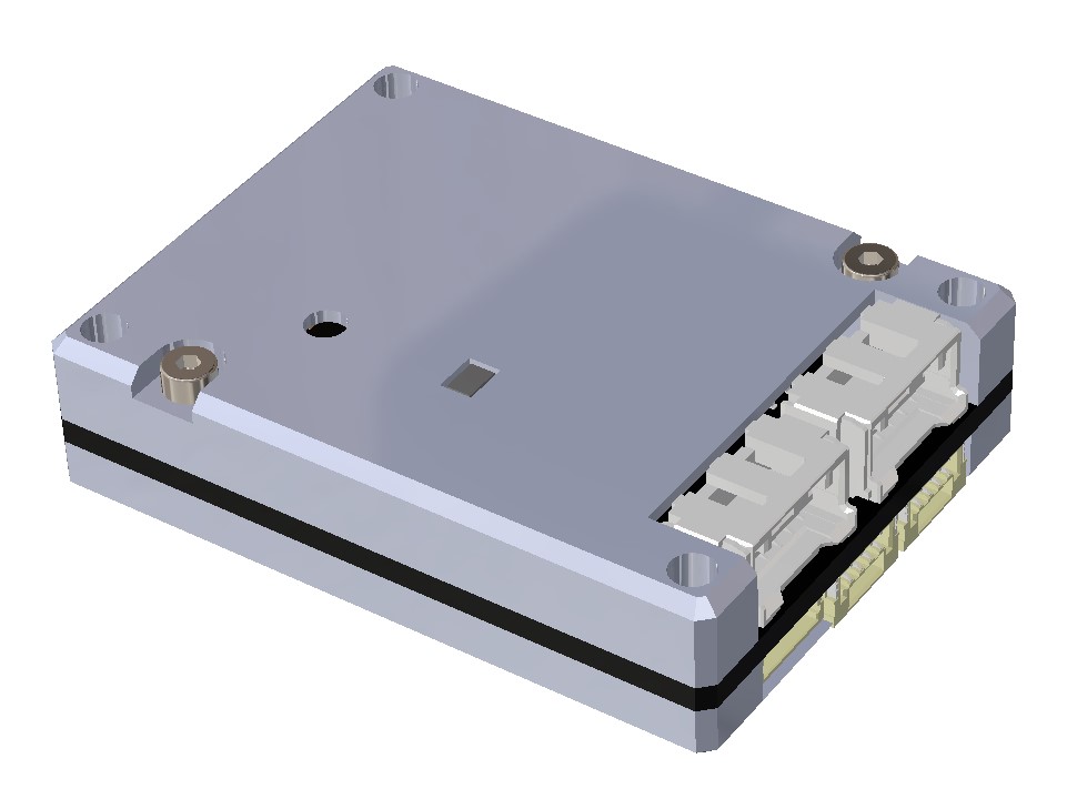
Scheme is shown on the picture below. CAN model can be provided via email request or issue on github or downloaded on GrabCAD (opens new window).

| Width, mm | Length, mm | Height, mm | |
|---|---|---|---|
| Outline | 52 | 39 | 13.9 |
| PCB | 52 | 39 | 1.6 |
| Mount holes (D = 3.2 mm) | 46 | 33 |
Total weight of device less than 14 g.
# Housing
The casing can be downloaded from GrabCAD (opens new window) and printed in ABS or PLA plastic. The housing consists of two parts: top and bottom. It can be assembled using M2 L=10mm (opens new window) screws DIN 912 (ISO 4762) and Bras Hot Melt Insert Nut (opens new window). The assembled unit can be fixed with double-sided tape or with M2 L=12-20mm (opens new window) screws.
Bill of materials:
| Name | Qty | Comment |
|---|---|---|
| ABS or PLA plastic | ||
| M2 L=10mm (opens new window) screws DIN 912 (ISO 4762) | 2 | In case of double-sided tape mount type |
| Bras Hot Melt Insert Nut (opens new window) | 2 | |
| Double-sided tape | ||
| M2 L=12-20mm (opens new window) screws DIN 912 (ISO 4762) | 4 | In case of screws |
Absolute Maximum Ratings
| Parameter | MIN | MAX | UNIT |
|---|---|---|---|
| Vin | 5.5 | 55* | V |
| V | 4.5 | 5.5 | V |
| I max | A | ||
| Operating temperature |
*Noted Voltage should be delivered only with current limitation under 2.5 Amp.
Recommended operating conditions
| Parameter | Value | UNIT |
|---|---|---|
| Vin (CAN3) | 30 | V |
| V (CAN1, CAN2) | 5 | V |
| I max | A |
ESD ratings
| Description | Value | UNIT |
|---|---|---|
| Human-body model (HBM) | 2000 | V |
| Charged-device model (CDM) | 500 | V |
# MTFF
# Integration
# Recommended mechanical mounting
# Functional Block Diagram
# Connection example diagram

# 3.5. Power Supply Recommendations
Device is designed to operate from an input voltage supply range between 4.5 V and 5.5 V over CAN1 or CAN2 connector, or 5.5 - 30 V from CAN3,CAN4. This input supply must be able to withstand the maximum input current and maintain a stable voltage. The resistance of the input supply rail should be low enough that an input current transient does not cause a high enough drop that can cause a false UVLO fault triggering and system reset. The amount of bulk capacitance is not critical, but a 47-μF or 100-μF electrolytic capacitor is a typical choice.
# 3.6. Revision history
| version | Description |
|---|---|
| v3.2.0 (opens new window) | Initial design |